Effect of Bypass Capacitor Placement and Layer SwitchingKim Flint, 8/12/2003
|
||||
| These simulations were done to show the effect of a signal switching layers. The signal changes reference planes as it switches. Different bypass capacitor locations, plane spacings, and board sizes are compared to see the effect.
Simulations were done using Speed2000 demo version from Sigrity. All the simulation files used here are available if you wish to try them yourself, or modify them for different cases. Click Here to download them. Since they were all done with the demo of Speed2000, anybody should be able to download the demo from Sigrity and use the simulation files. The Sigrity demo is limited in its functionality, but useful for looking at a simple example case like this. It is really interesting to watch the simulations. Speed2000 shows an animated 3d view of the voltage between the planes. As the signal passes through the via it is like a pebble landing in a pond. You see the wave propagate out from the via and bounce back and forth across the planes. Such a wave is of concern since it can result in crosstalk, EMI, or noise problems, so we would like to limit it as much as possible. The point of these simulations is to see what effect different capacitor placements have on minimizing the voltage difference between the planes, and compare it to using interplane capacitance. We expect that as the signal is travelling over a plane, its return current is flowing on the reference plane under it. As the signal switches from one side of the board to the other through the via, it changes the plane reference. The return current must also find a way to switch planes. This will happen by ac coupling between capacitance between planes. We can help this by placing decoupling capacitors on the board and by increasing the interplane capacitance with closer spacing between planes.What has the biggest effect? Stackup in all cases is Signal - Plane - Plane - Signal. Traces are 5 mil width, 5 mil height above planes. Dielectric is FR-4, Er=4.3 and loss tangent = .02. Two different cases of plane separation are simulated, 3 mil separation and 50 mil separation. 3 mil separation might represent a typical "power - ground sandwich" used in many modern PCB designs. 50 mil plane separation might represent the typical case of a 4 layer board, or planes separated by many layers in a larger layer count board. The demo version on Speed2000 is limited to 4 layers. With a full version it would be useful to use many layers and compare that as well. Two board sizes were used, 4" x 4", and 10" x 10". A larger plane of course means larger inter-plane capacitance. The smaller size could represent smaller boards, or a voltage island in a plane on a larger board with multiple voltages in use. The signal is generated by a current source with a 60 ohm resistor in parallel for the source impedance. It generates a 50mA pulse with 100ps rise and fall times, and 300 ps long at the top. You might want to try other waveforms. The signal generation itself does not disturb the voltage planes, which is different from how you might expect a real i/o to work but useful for seeing the effect of just the signal. The trace is microstrip, about 2.5" long. At the midpoint of the trace is a via, where the trace transitions from the top side to the bottom side of the board. The line is terminated with a 60 ohm resistor. The capacitor is taken as a lumped element with .1uF capacitance, 1nH inductance, and .1ohm resistance in series. These values of course vary with different capacitors available and different mounting techniques, and this is a bit of a worst case. You might want to try others. Three different cases of capacitor placement were considered. Close (500 mils) to the via, Far from the via (2.7" in the 4x4 board, 10.5" in the 10x10 board), and no cap at all. You might want to try other placements or multiple capacitors to see the effect. The plots below show distributions of the peak voltages between planes across the board area. The x-axis is volage, the y-axis is the number of points that reached that voltage. Having more points in lower voltages would be considered better. |
||||
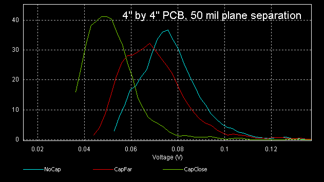
Plot 1.4" by 4" PCB. 50 mil plane separation. Three capacitor options: 500 mils from via, 2700mils from via, and no cap. This a distribution plot showing the peak voltages across the PCB planes vs. the number of measurement points reaching that voltage. Here we see the capacitor placement has a significant effect. If you do not have closely spaced planes or must switch across planes separated by many layers where there is not much interplane capacitance, bypass capcitor placement appears to make a difference. |
||||
 |
||||
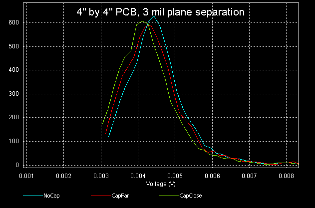
Plot 24" by 4" PCB. 3 mil plane separation. Three capacitor options, 500 mils from via, 2700mils from via, and no cap. Here we see the capacitor placement has a small effect, but not nearly as significant as with the larger plane spacing. We have much better interplane capacitance here to manage the return currents, which does a better job than our discrete capacitor. |
||||
 |
||||
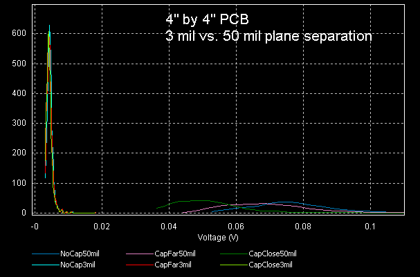
Plot 3Here are the two plots from above combined together to make the relative difference between them obvious. The 3 mil plane plots are the ones on the left, with much lower peak voltages across the board than the 50 mil plane spacings. |
||||
 |
||||
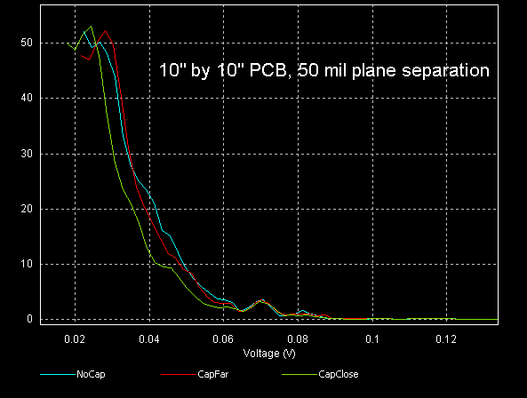
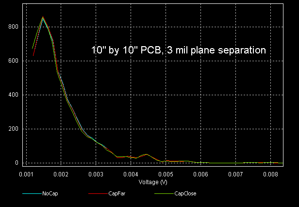
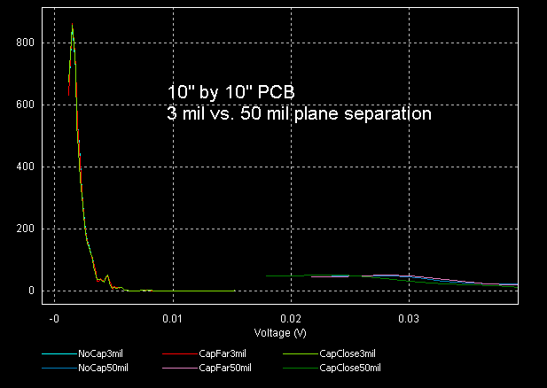
Plot 4, 5, 6These are similar cases to above, but using a 10" by 10" PCB. The "cap far" case now has the cap 10.5" away from the via. Here we see cap placement has less effect than the 4" board, but it still makes some difference for the 50 mil plane spacing. At 3 mil spacing it doesn't make a difference at all, presumably due to the large capacitance now formed between the two planes dominating. Once again, the biggest effect happens by switching layers through closely spaced planes. |
||||
 |
||||
 |
||||
 |
||||